PLEASE NOTE: If you had an account with the previous forum, it has been ported to the new Genetry website!
You will need to reset the password to access the new forum. Click Log In → Forgot Password → enter your username or forum email address → click Email Reset Link.
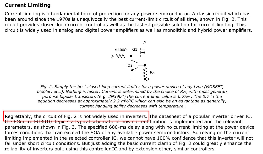
To truly test your inverters you need to put several in a chamber at least 120 degF, put them at full load, and let them soak until they stabilize at max internal temperatures. Then repeatedly hard short the outputs, at least 10 times. If they survive that you are ready for prime time.
Also a link to a paper on inverter reliability: http://www.how2power.com/newsletters/2201/articles/H2PToday2201_design_RedHillLabs.pdf?NOREDIR=1
Paper is titled: "Improving Solar Inverter Reliability: Techniques For Protecting Output Power Switches"
Jerry Steele
AKA Red Hill Labs
jerrysteele@redhilllabs.com
Paper is titled: "Improving Solar Inverter Reliability: Techniques For Protecting Output Power Switches"
WOW . MY Powerjack inverter will only run one and half hour before shut down at 120 degree F with 7 fans that sound like a 747 in my back yard . Powerjack will never use your moffets protection circuit . My PJ is useless in the summer . Thank you for your circuit design .
Then repeatedly hard short the outputs, at least 10 times. If they survive that you are ready for prime time.
That's more of a textbook example on "how to destroy something."
I read your PDF. The following quote seems to be the basis for your paper:
Well, there's a good reason said circuit is not used in power inverters.
Firstly, it's completely impractical. Secondly, it won't work in the way you think--said circuit is guaranteed to result in fried FETs.
Thirdly, a 100-ohm gate resistor is simply laughable: that alone is asking for a "rapid unscheduled FET disassembly." Not only will the rise/fall times be absolutely horrid (requiring increased dead-time to avoid H-bridge shoot-through), this also provides basically zero protection against Miller spikes--which are an absolute FET killer if not handled. Been there, done that...
Depending on how heavy the FET gate is ("Input Capacitance"), you will need closer to 10 ohms or less on the gate resistor PER FET. Couple that with a strong FET driver, and the transistor circuit's issues are just starting.
If I break it down:
The first issue is a compound problem. Depending on the transistor, Rcl (current sense resistor) may have to drop upwards of 1.2v to fully turn the transistor on. Simple Ohm's Law will show you that 1.2v * 100A = 120W of heat (if we design for 100A to be the "current limit" of a 135A-rated FET). Multiply that per each parallel FET (for a 6kw GS inverter, that's 6 per board) means that we now have a heat dissipation requirement of 720W at the current limit.
Wait, that's just for the low quadrant of the H-bridge--because the high quadrant needs the same circuit duplicated again (as the power flow through an H-bridge is diagonal). So we now have 1,440W of heat dissipation at the current limit. Let's not mention the catastrophic loss of efficiency this will result in, shall we?
The second issue is ALSO a compound problem. "Nothing is faster" than a bipolar transistor? This is completely false: a "high speed" switching transistor with any sort of current rating moves on molasses when compared to a run-of-the-mill high-current MOSFET. Put another way: a bipolar transistor is uselessly slow when put up against a MOSFET. I know this from experience: I tried making an active Miller clamp with a bipolar transistor (just this year actually)--which failed miserably. Why? The transistor is so slow that the Miller spike is already over and long gone BEFORE the transistor even starts to turn on. And to even reach the switching times specced on the transistor datasheet requires significant current into the base. (A 2SA1213 "high speed switching" PNP is rated ~1uS turn-on. The NCEP039N10 FETs we use have a turn-on time of 31.5nS [0.0315uS]--more than 30 times faster than the transistor. I ended up designing with a high-speed switching FET that turns on in a blistering 5.5nS, or almost 200 times faster than the transistor.)
The real issue? That shown transistor circuit is literally a linear current limit. The transistor will turn the FET off just enough to reduce the current to the design threshold. It will NOT turn the FET all the way off. This will put the FET into 100% linear mode at the full 100A limit--meaning that we have just flown well off the end of the FET's SOA chart, and melted the FETs right off the PCB.
If there's one thing a high current FET cannot handle, it's linear operation. This "Holy Grail" circuit's "protection mode" IS linear operation.
In short: you're better off with no current limit than with this circuit. This circuit will melt FETs at the current limit--it will not protect them.
The "improved" design with added resistors has the noted issue of "latching"--which of course becomes significantly exacerbated with the necessary 10-ohm gate resistors on the FETs. Let's not even think of mentioning the transistors' HFE/temperature curve (where the warmer a transistor is, the higher it's gain becomes) AND the battery voltage range...both of which will be very happy to run the circuit into latch-up, and bring the whole show to a quick end.
The UCC5870 chip is of slight interest, though with some notable shortcomings:
- One chip alone costs significantly more than a dozen FETs ($14/ea)
- There are no distributors in the U.S. that stock it right now (like most U.S. designed chips, it seems)--though it does have a comparatively quick 18-week lead time.
- Desaturation protection is basically useless on low-resistance low-voltage FETs. It's only usable on (comparatively) high-resistance IGBTs / high voltage FETs.
- this is because the voltage drop on a low voltage FET (at maximum current) is so low (easily <1v), compared to the wide forward voltage range of the diode in the desat circuit--which is quite dependent on ambient temps and current flow through the diode. IGBT desat can easily reach 6-8v, well beyond the forward voltage range of the diode.
The transistor is so slow that the Miller spike is already over and long gone BEFORE the transistor even starts to turn on. And to even reach the switching times specced on the transistor datasheet requires significant current into the base. (A 2SA1213 "high speed switching" PNP is rated ~1uS turn-on. The NCEP039N10 FETs we use have a turn-on time of 31.5nS [0.0315uS]--more than 30 times faster than the transistor. I ended up designing with a high-speed switching FET that turns on in a blistering 5.5nS, or almost 200 times faster than the transistor.)
Sean mention Miller spike on one of his youtube video and that only NCEP039N10 FET will work with 12kw or higher wattage inverter . All other FETs are too slow and blow up . Will Sean be able to get a supply of NCEP039N10 FET for your 12kw GS ? Sean say you make the mainboard in the USA to replace the one he blow up or will all the future mainboard be made by PJ for the pre-order ? No inverter can run continuous at 120 degree F so Sean do not have to test at that temperature .
Sean mention Miller spike on one of his youtube video and that only NCEP039N10 FET will work with 12kw or higher wattage inverter . All other FETs are too slow and blow up . Will Sean be able to get a supply of NCEP039N10 FET for your 12kw GS ?
It's not a matter of FET speed causing the blowups; rather, the NCEP039N10 FETs have a very low "reverse transfer capacitance" specification--meaning that the Miller spike is quite small. It still can't be ignored...but it DOES function, if *just*.
The NCEP039N10M FETs that I tried have a notably higher "reverse transfer capacitance" spec--and they blow like firecrackers at 3kw as a result. That's why I've been working on an active Miller clamp solution--so we aren't limited to just 1 or 2 FET options. It'll help the NCEP039N10 FETs as well...
Sean say you make the mainboard in the USA to replace the one he blow up or will all the future mainboard be made by PJ for the pre-order ?
I'm still prototyping designs, so the mainboard he'll get will be from me...but once the design is nailed down, it'll be manufactured by PJ for the pre-orders.
No inverter can run continuous at 120 degree F so Sean do not have to test at that temperature .
It's not impossible to design an inverter to run at 120F ambient--though the higher the ambient temperature, the less of a temperature difference there is before a critical threshold is reached. And the less of a temperature difference, the harder it is to dissipate waste energy. Depends what the design requirements are.
On 4/19/2022 at 7:38 AM, Sid Genetry Solar said:That's more of a textbook example on "how to destroy something."
I read your PDF. The following quote seems to be the basis for your paper:
<a class="ipsAttachLink ipsAttachLink_image" data-fileext="png" data-fileid="1290" href="/monthly_2022_04/image.png.725e87d6141a9c2ee9168b6731a08e09.png" rel=""><img alt="image.thumb.png.bcd1c5a93d60a56911bbfc69ba388e6e.png" class="ipsImage ipsImage_thumbnailed" data-fileid="1290" data-ratio="58.60" style="height:auto;" width="1000" data-src="//content.invisioncic.com/g308908/monthly_2022_04/image.thumb.png.bcd1c5a93d60a56911bbfc69ba388e6e.png" src="/applications/core/interface/js/spacer.png" />
Well, there's a good reason said circuit is not used in power inverters.
Firstly, it's completely impractical. Secondly, it won't work in the way you think--said circuit is guaranteed to result in fried FETs.
Thirdly, a 100-ohm gate resistor is simply laughable: that alone is asking for a "rapid unscheduled FET disassembly." Not only will the rise/fall times be absolutely horrid (requiring increased dead-time to avoid H-bridge shoot-through), this also provides basically zero protection against Miller spikes--which are an absolute FET killer if not handled. Been there, done that...
Depending on how heavy the FET gate is ("Input Capacitance"), you will need closer to 10 ohms or less on the gate resistor PER FET. Couple that with a strong FET driver, and the transistor circuit's issues are just starting.
If I break it down:
The first issue is a compound problem. Depending on the transistor, Rcl (current sense resistor) may have to drop upwards of 1.2v to fully turn the transistor on. Simple Ohm's Law will show you that 1.2v * 100A = 120W of heat (if we design for 100A to be the "current limit" of a 135A-rated FET). Multiply that per each parallel FET (for a 6kw GS inverter, that's 6 per board) means that we now have a heat dissipation requirement of 720W at the current limit.
Wait, that's just for the low quadrant of the H-bridge--because the high quadrant needs the same circuit duplicated again (as the power flow through an H-bridge is diagonal). So we now have 1,440W of heat dissipation at the current limit. Let's not mention the catastrophic loss of efficiency this will result in, shall we?
The second issue is ALSO a compound problem. "Nothing is faster" than a bipolar transistor? This is completely false: a "high speed" switching transistor with any sort of current rating moves on molasses when compared to a run-of-the-mill high-current MOSFET. Put another way: a bipolar transistor is uselessly slow when put up against a MOSFET. I know this from experience: I tried making an active Miller clamp with a bipolar transistor (just this year actually)--which failed miserably. Why? The transistor is so slow that the Miller spike is already over and long gone BEFORE the transistor even starts to turn on. And to even reach the switching times specced on the transistor datasheet requires significant current into the base. (A 2SA1213 "high speed switching" PNP is rated ~1uS turn-on. The NCEP039N10 FETs we use have a turn-on time of 31.5nS [0.0315uS]--more than 30 times faster than the transistor. I ended up designing with a high-speed switching FET that turns on in a blistering 5.5nS, or almost 200 times faster than the transistor.)
The real issue? That shown transistor circuit is literally a linear current limit. The transistor will turn the FET off just enough to reduce the current to the design threshold. It will NOT turn the FET all the way off. This will put the FET into 100% linear mode at the full 100A limit--meaning that we have just flown well off the end of the FET's SOA chart, and melted the FETs right off the PCB.
If there's one thing a high current FET cannot handle, it's linear operation. This "Holy Grail" circuit's "protection mode" IS linear operation.
In short: you're better off with no current limit than with this circuit. This circuit will melt FETs at the current limit--it will not protect them.
The "improved" design with added resistors has the noted issue of "latching"--which of course becomes significantly exacerbated with the necessary 10-ohm gate resistors on the FETs. Let's not even think of mentioning the transistors' HFE/temperature curve (where the warmer a transistor is, the higher it's gain becomes) AND the battery voltage range...both of which will be very happy to run the circuit into latch-up, and bring the whole show to a quick end.
The UCC5870 chip is of slight interest, though with some notable shortcomings:
- One chip alone costs significantly more than a dozen FETs ($14/ea)
- There are no distributors in the U.S. that stock it right now (like most U.S. designed chips, it seems)--though it does have a comparatively quick 18-week lead time.
- Desaturation protection is basically useless on low-resistance low-voltage FETs. It's only usable on (comparatively) high-resistance IGBTs / high voltage FETs.
- this is because the voltage drop on a low voltage FET (at maximum current) is so low (easily <1v), compared to the wide forward voltage range of the diode in the desat circuit--which is quite dependent on ambient temps and current flow through the diode. IGBT desat can easily reach 6-8v, well beyond the forward voltage range of the diode.
Thanks for your response. Much of your technical claims are "not even wrong".
Oh by the way, I have inverters here in Arizona (to clarify: the hottest desert in Arizona in the Harquahal Valley) that run at over 120 deg F continously several hours a day every summer and have since 2010.
IRF250 at 48 volts and 30 amps turns on in 750ns and turns off in 660ns with 100 ohms in the gate. If that's too slow then 50 ohms turns on in 430ns and off in 360ns. My reference to how fast the bipolar is a "relative" comment referring specifically to this circuit as there isn't any other practical device to use there. If you want to see a company who has proven this circuit in linear and switching IC's check out Apex Microtechnology. You fail to realize this circuit only needs to clamp the current until it gets the inevitable turn off pulse coming from your controller. Otherwise it lives there doing nothing. By the way I do like the fact you use an output transformer. Definitely a plus.
It is a fact that inverter reliability needs improvement. Welcome to the club.
Oh, and on the bipolar transistor. Any veteran of bipolar transistor design designs circuit where beta is irrelevant, and that is true here. As well as any beta drift. The base emitter voltage of something like a 2N3904 has been proven over years of use in this circuit to be centered at 0.7 volts at 25 degC. As far as temperature, all bipolar bases exhibit a -2.2mV/deg C tempco which insures that the current limit decreases with temperature to about 70% of its 25 degC value when it reaches 125 degC. Haven't you ever seen those temperature sensing IC"s that connect to a 2N3904 used as a temperature sensor and provide accurate temperature readings without calibration?
I'll try and quit bothering you now. I need to make plans for inverter purchases for myself and a few clients in the coming months.
Oh by the way, I have inverters here in Arizona (to clarify: the hottest desert in Arizona in the Harquahal Valley) that run at over 120 deg F continously several hours a day every summer and have since 2010.
Your inverters may run at 120 degree F for several hours but not connected to a 4 ton heat pump ? Your inverter must not be Powerjack inverter ? My Powerjack will run continously several hours at 120 degree F IF NO inductive load is connected but will only run one hour with 4 ton heat pump .
You fail to realize this circuit only needs to clamp the current until it gets the inevitable turn off pulse coming from your controller. Otherwise it lives there doing nothing.
I think someone other than me is overlooking a couple elephants in the room. Your "protection" circuit uses a fundamentally fatal design flaw as the basis for its existence.
As a baseline, the IRF250 (ancient dinosaur of a FET!) has a rated "Rds(on)" of 85mOhm (0.085 ohms), and rated maximum continuous current of 30A @ 25C. (I won't mention that the GS inverter FETs are 3.5mOhm [0.0035 ohms] with a rated current of 180A @ 25C [limited by package leads to 100A].)
With Ohm's Law, we can determine that 30A through a 0.085 ohm resistance will dissipate 76.5W, dropping 2.55v. If we are pulling 30A from a 50v supply, then the "load" resistance will be (50 - 2.55v = 47.45v across the load with 30A) = 1.582 ohms, resulting in 1,423W dissipation in the load. Total equivalent circuit resistance is 1.667 ohms.
But let's say we have an overload condition, and the total circuit current increases to 90A @ 50v. Load resistance drops to 0.47 ohms--and this factor becomes extremely important. This "protection" circuit will activate, and pull the MOSFET gate down just far enough to drop the DC current through the circuit to 30A. So far, so good...the MOSFET max continuous current is 30A, so we're good, right? Well...only if you overlook any further calculations.
So let's recalculate now. For 30A at 50v, the circuit resistance is determined by Ohm's Law to be 1.667 ohms. But due to the overload condition, the "load" is 0.47 ohms. This means that in order to drop the circuit current to 30A, the MOSFET must fill in the remaining resistance of (1.667 - 0.47) = 1.197 ohms. Here's where it all goes wrong: 1.197 ohms @ 30A = 1,077W of heat that WILL be dissipated in the FET. But the datasheet lists the maximum dissipation of the IRF250 as 150W--this is where the FET is going to explode. While the FET package does have some mass, the real issue is the RthJC specification--thermal dissipation between the junction and case, of 0.83C/W. So 1,077W of heat * 0.83 = 894C on the actual FET junction almost instantaneously (regardless of FET case heatsinking)...which guarantees instant failure.
Without the "protection" circuit, Ohm's law finds that 90A @ 0.085 ohm Rds(on) results in 688W dissipation in the FET. Still fatal for a 150W-rated FET--but not as bad as the "protected" FET circuit.
In order to actually protect FETs from an overcurrent condition, you need to clamp them all the way to full off (open circuit = no power flow). In normal modern motor controllers, this is generally done with a current sense comparator that shuts down PWM outputs down on the MCU. Depending on the implementation, this can be either until user intervention, or on a cycle-by-cycle basis.
For that matter, the "inevitable turn off pulse" is a completely useless argument--if it had any merit at all, there would not be any need for a protection circuit in the first place. Bottom line: "protecting" an overloaded FET by increasing it's heat dissipation is a rather effective way make a bigger smoke show. I guess if you're going to go out with a bang, you might as well make it a good one....
I think someone other than me is overlooking a couple elephants in the room. Your "protection" circuit uses a fundamentally fatal design flaw as the basis for its existence.
There is no way to try to make any of your inverter to run at 120 degree F in Arizona with any modify circuit The FETs will blow because your inverter is outside as seem in your video in the desert of Arizona . My Powerjack will not run in 120 degree F heat and I try many different way and now gave up .
There is no way to try to make any of your inverter to run at 120 degree F in Arizona with any modify circuit The FETs will blow because your inverter is outside as seem in your video in the desert of Arizona . My Powerjack will not run in 120 degree F heat and I try many different way and now gave up .
Remember, "Power Jack" is not the Webster dictionary's definition of an inverter.
It is quite possible to design an inverter to function at 120F ambient--simply the losses have to be less in order to avoid overheat.
58 minutes ago, dickson said:I think someone other than me is overlooking a couple elephants in the room. Your "protection" circuit uses a fundamentally fatal design flaw as the basis for its existence.
There is no way to try to make any of your inverter to run at 120 degree F in Arizona with any modify circuit The FETs will blow because your inverter is outside as seem in your video in the desert of Arizona . My Powerjack will not run in 120 degree F heat and I try many different way and now gave up .
That fatal flaw circuit is in millions of linear and switching power amplifier IC's, typical of those made by Apex technology. And you'll notice the TI MOSFET driver has provision for just such a current limiter. I guarantee there is a lifetime of experience behind what TI puts in their IC's. I should know, I defined many of them.
I think we can end this (endless) debate since there appears to be zero agreement on anything and it is really just a pissing contest. I do appreciate the engaging discussion and I truly do wish you luck in your endeavours.
I happen to drive pass Apex technology all the time . I do not think they make circuit for Chinese inverter . Thank you for the information .
.png.f932b65b9e0ffcc2cd867c2c8fb1feca.png)
.png.b6456bbe3127ecad87e504d4acdb111a.png)
1 hour ago, Red Hill Labs said:That fatal flaw circuit is in millions of linear and switching power amplifier IC's, typical of those made by Apex technology. And you'll notice the TI MOSFET driver has provision for just such a current limiter. I guarantee there is a lifetime of experience behind what TI puts in their IC's. I should know, I defined many of them.
I think we can end this (endless) debate since there appears to be zero agreement on anything and it is really just a pissing contest. I do appreciate the engaging discussion and I truly do wish you luck in your endeavours.
The circuit is fine for low voltage(<100V)/low power(<2kW) systems and used in many systems as you mentioned. However, it is impractical, at least not without modifications, for high voltage(>100V)/high power(>2kW) systems as <a contenteditable="false" data-ipshover="" data-ipshover-target="/profile/2-sid-genetry-solar/?do=hovercard" data-mentionid="2" href="/profile/2-sid-genetry-solar/" rel="">@Sid Genetry Solar explained. It would be educational, if you can provide examples of high voltage/high power systems using the circuit.
Most robust industrial high voltage/high power systems use desaturation over-current/short-circuit detection/shutoff circuits. Consumer systems usually use current sensing/detection circuit and shutoff by microcontroller in software which is not as fast and more likely to fry FET's/IGBT's under over-current/short-circuit conditions since most FET's/IGBT's have <10uS of short-circuit withstand time.
Consumer systems usually use current sensing/detection circuit and shutoff by microcontroller in software which is not as fast and more likely to fry FET's/IGBT's under over-current/short-circuit conditions since most FET's/IGBT's have <10uS of short-circuit withstand time.
Most MCUs designed with H-bridge PWM control will have a hardware path for cycle-by-cycle current limiting (including the MCU used in the GS inverters) with reaction times measured in nanoseconds.
And yes, I fully agree that software-controlled overcurrent protection is not much of a protection.
The circuit is fine for low voltage(<100V)/low power(<2kW) systems and used in many systems as you mentioned. However, it is impractical, at least not without modifications, for high voltage(>100V)/high power(>2kW) systems as @sid-genetry-solar explained. It would be educational, if you can provide examples of high voltage/high power systems using the circuit.
Fully agreed...the rules change significantly between low power systems and high power systems. "Oh, let's make a 12kw inverter, it's just double the size of a 6kw." Whew, was that an understatement! Transformer's DC current (i.e. short-circuit/saturated) goes from 3,000A in the 6kw (with FETs absolute max of 3,600A) to over 18,000A in the 12kw (and FETs at 5,940A absolute max)--now the FETs aren't intrinsically protected by the circuit's DC resistance anymore.
That fatal flaw circuit is in millions of linear and switching power amplifier IC's, typical of those made by Apex technology.
I'm not saying that the circuit is useless or even fatally flawed when used in the right application. It has useful applications in many fields--and is commonly used in analog designs and chips. Like you said, it's used in linear amplifiers and linear control circuits.
I am just saying that for high-current SPWM-driven inverters (with non-linear control), the "linear current limit circuit" is an unmitigated, total and complete disaster. If we should even think of running the FETs in linear range "to limit current at 1,100A", they are going to blow up--and that's a guaranteed end result. Been there, done that.
And you'll notice the TI MOSFET driver has provision for just such a current limiter. I guarantee there is a lifetime of experience behind what TI puts in their IC's. I should know, I defined many of them.
The UCC5870 datasheet shows sample circuits using the ADC inputs for current monitoring across a current sense resistor--but I did not see any examples of linear current limiting. Worth noting that "desaturation detection" will shut the FET/IGBT down, not run it further into linear state--otherwise you're guaranteed a blown FET/IGBT.
Didn't study the datasheet to see if it has automatic threshold cycle-by-cycle current limiting ability built-in or not (through digital shutdown)...but wouldn't be surprised if it did. Really powerful chip.